Contact Form

What Is Thin Film?What is thin film?
What Is Thin Film?
In this section, we will explain what thin film is.
Although the term may not be familiar to everyone, thin film is indispensable to our daily lives.

Thin film can be compared to a soap bubble.
By making the layer extremely thin—much thinner than conventional coatings such as paint or spray coatings—it interacts with light, creating a shimmering, rainbow-like appearance. The thickness of thin film is measured in nanometers (nm), which is approximately one-thousandth the thickness of a human hair. Thin film is produced by precisely controlling the thickness of each layer and stacking multiple layers sequentially.
Roles of Thin Film
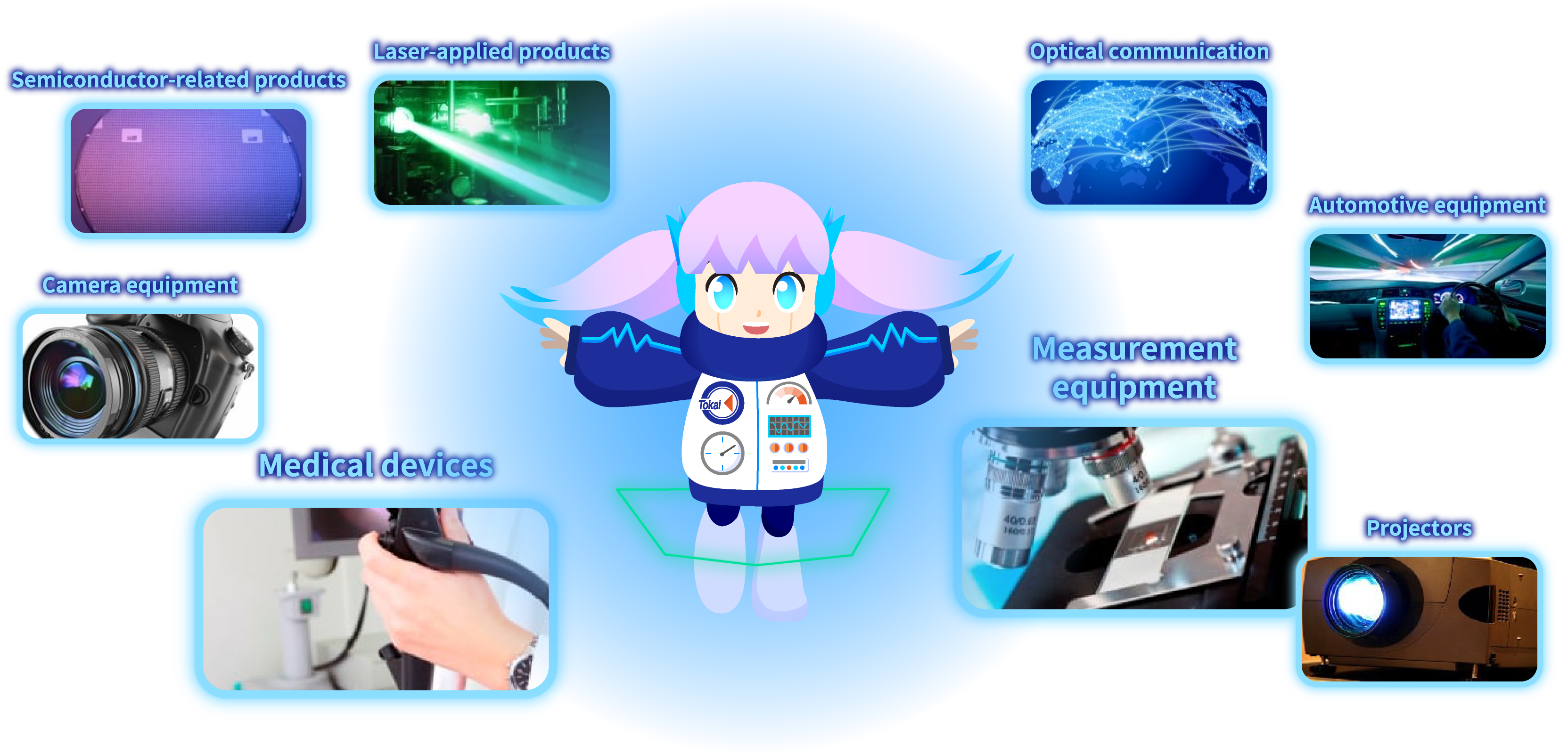
Thin film fulfills a wide range of roles depending on the materials used and their combination with base materials. Below are some representative examples.
These films reduce the reflection of light. They are widely used in devices such as smartphones and fiber for optical communication.
These films selectively transmit or reflect light within specific wavelength ranges. They are used in applications such as thermal detection devices and infrared sensors.
These films repel substances that adhere to the surface. There are various types, including water-repellent, antibacterial, and anti-fouling films.
These films allow light to pass through while also conducting electricity. They are commonly used in applications such as smartphone touch panels.
These filters reduce the intensity of transmitted light while suppressing visible light reflection. They are used, for example, in professional movie and video recording cameras.
How Thin Film Is Formed
What Is Vacuum Deposition?
Vacuum deposition is a thin film processing technique in which materials such as metals or metal oxides are heated in a vacuum environment and caused to evaporate or sublimate.
The evaporated or sublimated particles (atoms or molecules) then adhere to or are deposited onto the surface of a substrate, forming thin film.
Common examples of this technology include anti-reflection coatings and blue light cut coatings applied to eyeglass lenses, which may be familiar to many people.
Thin film processing by vacuum deposition is carried out in a vacuum environment because the presence of water molecules in the air would interfere with the vaporized material particles.
This interference can reduce film adhesion and lead to deterioration in film quality.

Principle of Vacuum Evaporation
When water is placed in a pot and heated, it turns into water vapor and evaporates.
If a substrate is placed above the vapor, the water vapor adheres to the surface and forms a thin layer of water.
Vacuum evaporation applies the same principle, but instead of water, materials such as metals or metal oxides are heated and vaporized.
The vaporized material then reaches the substrate surface and forms thin film.
Water boils at 100°C; however, in the case of metals or metal oxides, temperatures of several hundred degrees Celsius are required simply to melt the material, and temperatures of several thousand degrees Celsius are necessary to cause evaporation or sublimation.
For this reason, a vacuum environment is required, in which the pressure is reduced and the number of gas molecules is minimized.
The substrates onto which thin films are deposited are made of materials such as glass or resin and are mounted on umbrella-shaped fixtures known as “domes.”
Products such as substrates and lenses are set on these domes.
Our company owns a wide variety of domes and fixtures that can accommodate products of many different sizes.
- ●This method is suitable for materials with relatively low melting points.
- ●The thin film material is placed in a high-melting-point container made of molybdenum (Mo), tungsten (W), or tantalum (Ta). The container is then heated, causing the material to vaporize.
- ●This method is suitable for materials with high melting points.
- ●The thin film material is placed in a crucible, and an accelerated electron beam is directed onto the material, causing it to vaporize.
-
●This method is based on the electron beam method and improves film quality by irradiating the substrate with ionized gas particles generated by an ion gun.
By applying ion assist, the thin film becomes denser, exhibits stable properties without degradation caused by moisture, and achieves high adhesion, resulting in a high-quality film.
Sputtering Method
Not all materials can be formed into thin films using the vacuum evaporation method. In addition to vacuum evaporation, there is another thin film processing technique known as sputtering.
In sputtering, an inert gas such as argon is ionized, and the ionized particles are accelerated and made to collide with the target material. This collision ejects material particles, which then adhere to the substrate and form thin film. Compared with the vacuum evaporation method, sputtering enables thin film formation using materials with high melting points that are difficult to process by vacuum evaporation.
Sputtering also has the following characteristics:
●Strong adhesion between the thin film and the substrate
●Dense film formation resulting in high film quality and durability
●High reproducibility of the deposition process
●Faster deposition process compared to vacuum evaporation

Thin Film Patterning Using Photolithography
In addition to deposition techniques, various other technologies are also utilized in thin film processing.
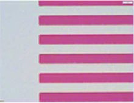
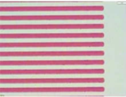
Forming a thin film into a specific shape is referred to as patterning. To create thin films with such patterns, a technique known as photolithography is used. At Tokai, we leverage photolithography to pattern optical multilayer films into a wide variety of shapes.
First, a resin that hardens or dissolves when exposed to light is applied to a substrate on which a thin film has already been formed. Light is then irradiated through a patterned mask, and the substrate is developed and washed, causing the resin to remain in the desired pattern.
Next, the thin film in areas not protected by the resin is removed. Finally, the remaining resin on top of the thin film is also removed, resulting in a thin film with the intended pattern.


By combining various thin film deposition techniques with photolithography processes, we are able to produce thin films with highly precise patterns.
At our company, we offer flexible support to meet our customers’ requirements by producing a wide range of materials and patterns.
We can achieve patterning precision of up to 1 μm.
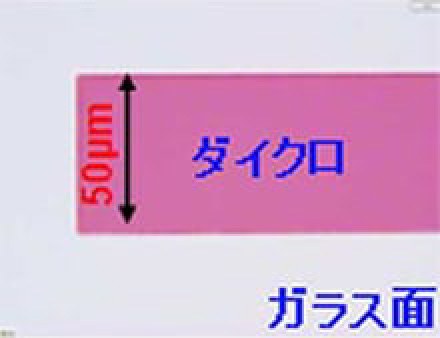 50μm
50μm
 10μm
10μm
 5μm
5μm
 2μm
2μm
 1μm
1μm
We can also arrange areas with different properties in close proximity.
● Pattern Examples
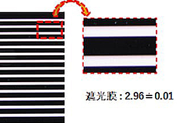
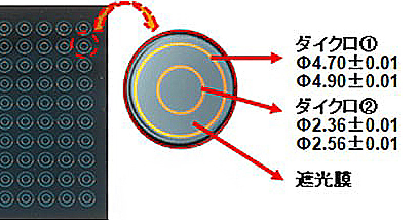 1.Dichroic Film & Light-Shielding Film
 2.ARMC & Light-Shielding Film
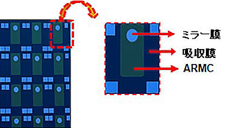 3.Mirror Film, Absorptive Film & ARMC
By combining various materials and patterns in this way, it is possible to create thin films with more complex and highly functional patterns.
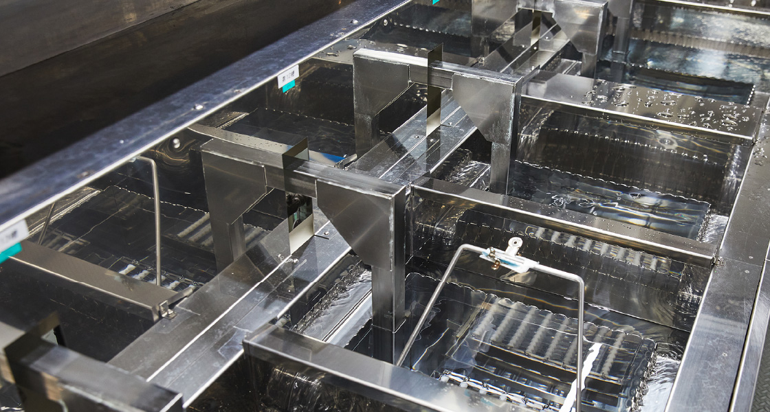
Precision Cleaning Technology
Cleaning is an essential technology in thin film processing.
Thin films are formed by attaching particles of various materials onto the surface of a substrate.
If the substrate surface is contaminated, it is not possible to produce a clean and high-quality thin film.
Many people apply protective films to the screens of smartphones or handheld gaming devices.
If dust remains on the screen when the film is applied, air bubbles may form, visibility may be reduced, or the film may peel off more easily.
The same issues can occur in thin films if the substrate is not properly cleaned.

First, contaminants on the substrate are removed using a combination of cleaning solutions and ultrasonic waves.
The cleaning solution is selected according to the type of contamination and the properties of the substrate, and may be alkaline, mildly alkaline, or neutral.

After cleaning, the cleaning fluid contains various chemical substances and residues of removed contaminants.
To remove these, the substrate is rinsed using pure water free of impurities.

Finally, drying is performed using a specialized liquid and equipment known as an IPA bath. For further information, please refer to Our Technologies: Precision Cleaning Technology.
Our efforts extend beyond the cleaning process itself.
Our efforts extend beyond the cleaning process itself.
To maintain consistent cleaning quality, we also place strong emphasis on the maintenance of our cleaning equipment.
Cleaning with contaminated equipment cannot achieve proper results.
Based on our many years of experience, we establish appropriate maintenance cycles and perform regular maintenance on our equipment.
Dicing Process
Small products are processed using a method known as dicing.
For products such as semiconductors that are difficult to process at their final size, fabrication is first carried out in a larger form. The material is then cut into individual product sizes. This cutting process is referred to as dicing.
At our company, dicing is primarily performed on glass-based substrates to create individual chips.
As a processing method, we use blade dicing, in which a thin grinding blade is rotated at high speed to precisely cut the substrate.

Thin film processed products manufactured in this way are assembled together with other components to deliver their intended performance.
At our company, this assembly process is carried out inside a cleanroom by skilled technicians who are experienced in handling optical components, ensuring a high level of quality in the finished products.
Thin films themselves are only very small components of the systems that incorporate them. However, the performance of thin films can enable more compact system structures and designs, as well as enable the addition of new functions beyond the original design requirements.
In this way, thin films contribute to enhancing the overall value of the system.
The Future of Thin Film
For example, more vehicles are now equipped with numerous sensors that issue warnings when a potential collision is detected.
As autonomous driving becomes commonplace, sensors with even higher performance will be required.
To achieve such high-performance sensors, advanced thin films will be essential.
Not only for sensors, our customers’ requirements have also become increasingly diverse, and we are now more frequently asked to produce thin films that we have never handled before.
New requirements and encounters with new materials lead to the evolution of thin film processing technology.
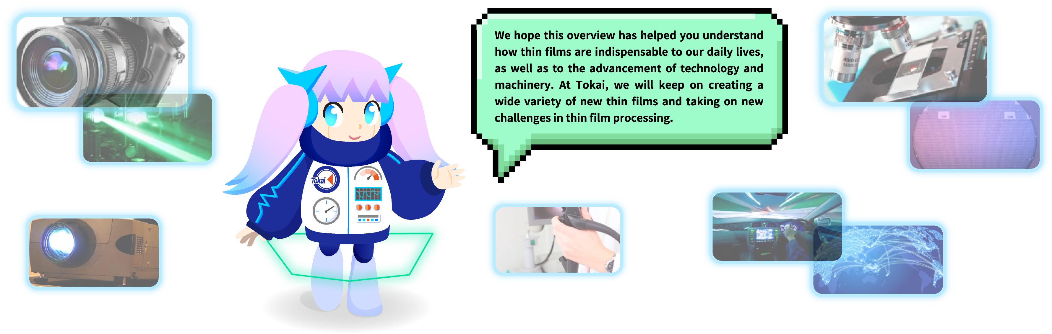
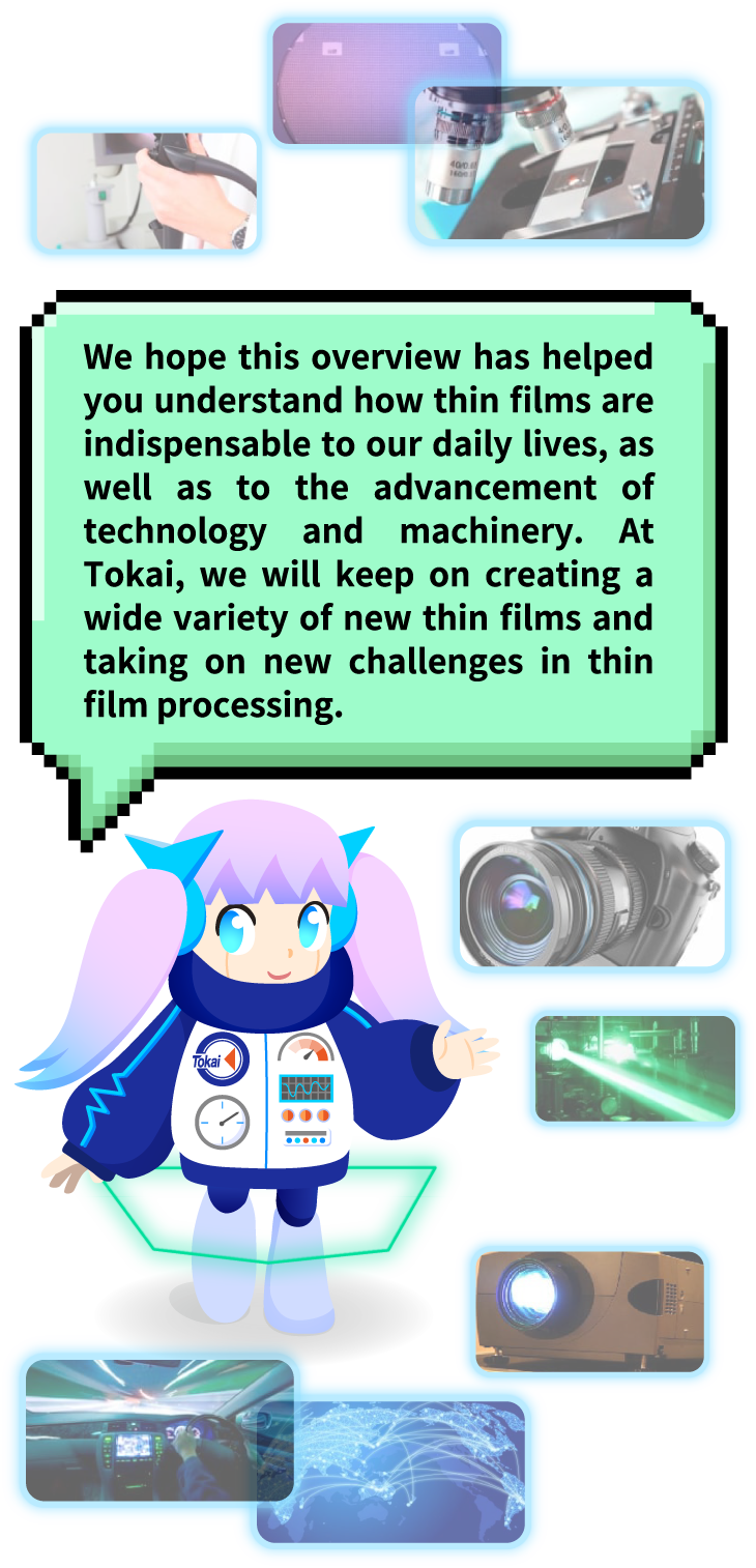
Through the ongoing development of thin film processing technologies, we hope to inspire ideas such as,
“If thin films like this can be created, entirely new types of systems and products—previously unimaginable—may become possible.”